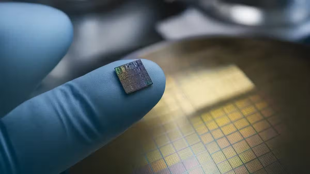
The IBM NanoStack Chip Technology has introduced a groundbreaking advancement that could reshape the future of semiconductor manufacturing. IBM recently unveiled what it describes as the world’s first chip technology below the 1-nanometer scale, capable of fitting nearly 100 billion transistors onto a chip roughly the size of a fingernail. This innovation represents a major leap forward in chip design and could significantly improve computing performance, power efficiency, and artificial intelligence capabilities over the coming years.
As demand for faster processors and more powerful AI systems continues to grow, IBM’s latest breakthrough demonstrates that chip innovation is far from reaching its limits.
A New Approach to Chip Design
Unlike traditional chip manufacturing methods that primarily reduce transistor sizes across a flat surface, IBM NanoStack Chip Technology introduces a three-dimensional architecture.
The technology stacks transistors vertically instead of placing them only side by side. This design allows engineers to fit many more transistors into the same physical area while maintaining high performance and improving energy efficiency.
By moving chip scaling into three dimensions, IBM believes it can continue advancing semiconductor technology well beyond current manufacturing limitations.
What Is NanoStack?
NanoStack is IBM’s advanced transistor platform built around vertically stacked nanosheet transistors.
Instead of using a single transistor layer, the system combines two transistor structures into one vertical arrangement. Each layer can use different semiconductor materials, metals, and insulating components depending on performance requirements.
This flexibility allows engineers to optimize individual transistor layers independently while improving the overall performance of the chip.
The result is a platform designed not only for today’s manufacturing processes but also for future generations of semiconductor development.
Nearly 100 Billion Transistors
One of the most impressive achievements of IBM NanoStack Chip Technology is its extraordinary transistor density.
IBM’s prototype can accommodate nearly 100 billion transistors on a chip approximately the size of a human fingernail.
For comparison, many of today’s most advanced processors contain around 80 billion transistors.
Higher transistor density allows processors to perform more calculations simultaneously, improving computing speed while enabling increasingly sophisticated workloads.
This development could benefit everything from smartphones to high-performance servers.
Better Performance With Less Power
Power efficiency remains one of the biggest challenges facing modern computing.
According to IBM, NanoStack can deliver up to 50% higher performance compared to its earlier experimental 2nm technology while using the same amount of energy.
Alternatively, the technology can reduce power consumption by as much as 70% while maintaining similar performance levels.
Lower power requirements translate into longer battery life for mobile devices, lower operating costs for data centers, and reduced environmental impact through lower electricity consumption.
Benefits for Artificial Intelligence
Artificial intelligence places enormous demands on modern processors.
AI training and inference require high-speed memory access, large processing capacity, and efficient data movement across chips.
IBM NanoStack Chip Technology addresses these challenges by improving static random-access memory (SRAM) density by approximately 40% compared to previous designs.
Greater on-chip memory allows processors to store more information close to computing units, reducing delays caused by transferring data across different parts of the system.
This improvement could significantly accelerate AI workloads while increasing overall system efficiency.
Preparing for the Angstrom Era
IBM views NanoStack as more than a single manufacturing breakthrough.
The company believes the technology can evolve through several future process generations, eventually reaching manufacturing scales measured in angstroms rather than nanometers.
An angstrom represents one ten-billionth of a meter, making it ten times smaller than a nanometer.
Moving toward angstrom-scale manufacturing could extend semiconductor innovation for another decade while supporting increasingly complex computing applications.
Applications Across Multiple Devices
The potential uses of IBM NanoStack Chip Technology extend far beyond desktop processors.
IBM expects the architecture to eventually support:
- High-performance CPUs
- Graphics processors (GPUs)
- Smartphone processors
- Artificial intelligence accelerators
- Advanced memory chips
- Data center hardware
Because the platform improves both speed and efficiency, it offers benefits across consumer electronics, enterprise computing, cloud infrastructure, and scientific research.
Production Timeline
Although NanoStack remains an experimental technology, IBM believes commercial production could begin within the next five years.
As manufacturing techniques mature, semiconductor companies may adopt similar three-dimensional transistor designs for future chip generations.
While bringing new semiconductor technologies into mass production requires extensive engineering and investment, IBM’s research demonstrates that continued innovation remains possible despite the growing complexity of modern chip fabrication.
The semiconductor industry constantly searches for new methods to improve performance while reducing power consumption.
Traditional transistor scaling has become increasingly difficult as components approach atomic dimensions.
By introducing a fundamentally different architecture, IBM NanoStack Chip Technology provides a new roadmap for future semiconductor development.
If successfully commercialized, this innovation could support faster artificial intelligence systems, more powerful smartphones, improved cloud computing, and next-generation scientific research.
The IBM NanoStack Chip Technology represents one of the most significant semiconductor breakthroughs in recent years. Through its innovative three-dimensional transistor architecture, IBM has demonstrated that chip performance and efficiency can continue improving even as traditional manufacturing approaches reach their physical limits.
With nearly 100 billion transistors, substantial performance gains, improved memory density, and lower energy consumption, NanoStack offers a glimpse into the future of computing. As the technology moves closer to commercial production, it has the potential to redefine processor design and power the next generation of AI, mobile devices, and high-performance computing systems.